Medontech offers the most powerful PCB design services with the experienced engineering talents in the state-of-the-art tools & technologies that best utilize to deliver the high quality, cost effective design to meet our customer technical requirement& demanding schedules.
Our Top Notch PCB designers are IPC certified with the broad spectrum of expertise and knowledge; with decades of printed circuit board (PCB) experiences, we are exposed to wider variety of design challenges & on various cutting-edge technologies. Leveraging our experiences from the complex, high layer count, High speed Digital designs, power designs, RF design, Analog designs, mixed designs; we serve a wide variety of markets like Telecommunication & Networking, wireless, medical, automotive, Consumer electronics, data & storage systems, military, aerospace and many more.
We developed & employ the proven PCB design process & Quality checks for the complete design flow from the start to the manufacturing release to ensure the design meets all the specifications & to increase the efficiency. No matter what Printed circuit board (PCB) design program, the process is followed commonly for low to high complex PCB designs to ensure the best quality all times. We at Medontech, constantly develop, tune & use the custom programs to help achieve greater efficiencies & to improve quality by reducing the manual effort.
-
 PCB Design technologies
- High speed Digital designs, Analog designs, mixed designs, power designs & RF design
- Signal Integrity, EMC & EMI Compliant designs
- PCBs with DFM, DFT, DFA requirements
- PCBs for Pb-free, RoHS, EuP certifications
- PCBs with Controlled impedance requirements
- PCBs for mechanical constrained designs
- PCBs for Flexi, Rigid & Rigid-Flex designs
- PCBs for Mobile phone designs with ALIVH technology
- HDI designs with via-in-pad, blind via, buried via & micro vias
- Effectively used via stacking & staggering technology
- High frequency PCBs of up to 10Gbps
- High layer count PCBs of up to 38 layers
- Dense PCBs with pin count of 10000+ pins
- PCBs with high pin density of 540 pins/sq. inch
- High component count PCBs; > 6000 components
- Designs with fine pitch BGAs of 0.4mm & 0.5mm
- Designs with high pin count full matrix BGA 1422pins with 0.5mm pitch
- Designs with 3mils/3mils trace & spacing
-
Technologies on Board
- DDR3,DDR2,DDR,SAS,Rambus,SDRAM, QDR, Flash, CompactFlash
- GMII, XGMII, XAUI, POS-PHY Level3, POS-PHY Level4, SPI-4, SFI-4
- SONET/SDH, POE, GbE, 10GbE
- PCIe, PCIX,cPCI ,Rocket IO,
- VME, IDE, SCSI, iSCSI, PCMCIA, SDIO,LVDS,RVDS
- XAUI,SERDES,SPI-4,AGP
- USB, UART,I2C & I2S
- HDMI,DVI, Composite Video, S Video, VGA
- 4G LT WiMax / 802.11a,b,g & n
- Bluetooth, GPS & GPRS designs
- Designs with Intel based processors
- Designs for the Mobile phones
- Designs with FPGA & ASIC
- Designs with 3G & 4G technologies
- Designs with printed antennas
-
PCB Design Tools
-
Medontech Advantages
- Large pool of highly experienced IPC designers with expertise in multi tools & technologies
- Easy scale up of the resources as per the design requirements
- We will work around your schedule with flexible timings to meet your requirements
- More reliable and consistent in the quality of deliverables
- Extensive PCB design process & Quality checks
- Offer 24x7, 365 Days of design support
- On & Offsite design support
- Expert project management, open communication & Daily status reports
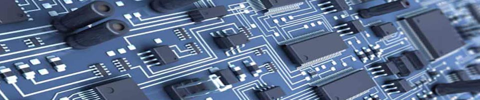
 PCB Design